V
主页
京东 11.11 红包
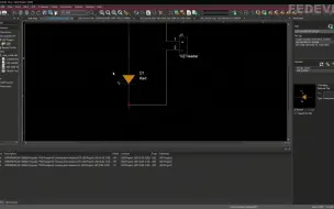
01-OrCAD and Cadence Allegro 示意图-005创建LED示意图符号
发布人
打开封面
下载高清视频
观看高清视频
视频下载器
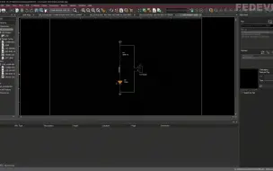
01-OrCAD and Cadence Allegro示意图-003创建1x2标头示意图符号
02-OrCAD and Cadence Allegro 足迹-007创建0805电阻器足迹.mp4
01-OrCAD and Cadence Allegro 示意图-006图纸示意图
02-OrCAD and Cadence Allegro 足迹-004创建VIA
02-OrCAD and Cadence Allegro Footprints-009修复警告并运行DRC
02-OrCAD and Cadence Allegro 足迹-003为LED创建SMD焊盘
03 OrCAD和Cadence Allegro PCB布局-006编辑示意图和更新PCB
03 OrCAD和Cadence Allegro PCB布局-001启动新PCB
02-OrCAD and Cadence Allegro 足迹-006创建0603 LED足迹.mp4
03 OrCAD和Cadence Allegro PCB布局-003设置规则和堆栈
03 OrCAD和Cadence Allegro PCB布局-002组件放置
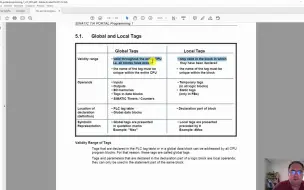
005 PLC标记、符号
从零开始制作四旋翼无人机 EP01 - 硬件原理图与PCB介绍
电路板线路图是怎么制作的?分享简单五步骤
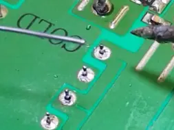
这焊接技术还可以吧
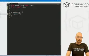
3.2.chatgpt python创建主页
Part2-800MHz 45W 射频功率放大器的快速实现
18.NX创建冷却销孔
开关电源TPS54302的5V输出电路设计
050 How to create a plan in CFD-Post,CFD-Post创建平面
starccm 基于脚本自动化网格检测,场景自动创建
4.5.chatgpt python 创建建议请求
LED电路中的电阻有什么作用
6.3.chatgpt python创建过去代码页
基于YOLOv8的PCB缺陷检测系统 结合小目标检测头与mpdiou损失函数 实现涨点2% 代码见评论区
【硬核】手搓电容屏-第一版
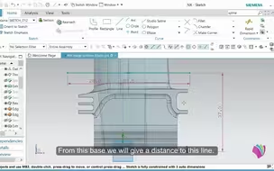
5-01-使用核心设计工具创建几何图形
手把手教你做【WIFI控制器】①:原理分析
第0讲 嵌入式物联网综合项目LoRa项目简介&准备
阻抗测试--求佛不如求自己
PCB锐角走线有啥危害?
【PCB布线秘籍】走线宽度的形象比喻“水管粗细”
宇宙魔方量产计划!
电路中芯片为什么要串联电阻
57-chatgpt创建第一个CSS页面
电子小白必知的12条常见PCB设计规范。#零基础教学 #硬件开发 #PCB设计 #硬件工程师
手把手教你做【WIFI控制器】⑦:代码怎么写?
HyperView HyperGraph 2022 第1~3章节
DDR内存芯片的PCB等长设计-1.走线等长参考 2.等长or等时
高频pcb板和普通pcb板有什么区别