V
主页
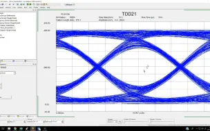
PLTS Operation (1-2. Parameter, Format, Scale, Marker)
发布人
打开封面
下载高清视频
观看高清视频
视频下载器
PLTS Operation (1-4. Equation, Intra Pair Skew)
PLTS Gating
PLTS Rise Time Setting
PLTS Operation (2-3. Calibration Wizard with ECal)
PLTS Operation (1-1. Opening File and DUT Port Config)
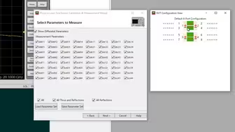
PLTS Operation (2-2. Measurement Wizard)
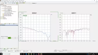
PLTS Operation (2-1. Start PLTS and get measured values)
PLTS Programming (Part1)
PLTS Operation (1-5. Port Assignment Procedure)
PLTS Operation (2-4. Probe calibration using PLTS)
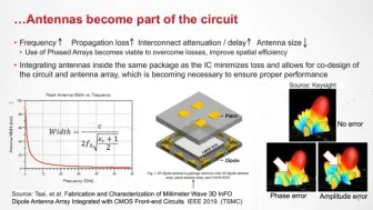
Latest Interconnect Trends in Commercial Grid-scale & Residential Energy Storage
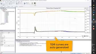
How to View TDR of An S Parameter Model Quickly
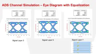
PLTS Operation (1-3. Eye pattern, Limit Line Test)
PLTS Programming (Part2)
S Parameter Master Class - Part 2
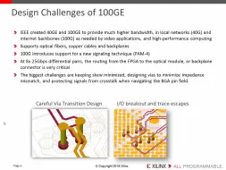
Designing to Win in 100G Ethernet
CST Tutorial - Cable Simulation
HFSS Tutorial_ Design of SMA Connector
How to Use Fixture De-embedding to Match Signal Integrity Simulations to Measure
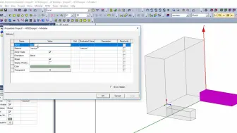
Differential Via Optimization with Ansys HFSS 3D Layout and Ansys optiSLang
Designing Wafer Level Chip Scale Packaging
Delta-L
High-Speed USB C & USB 3 PCB Design and Current Circuit Board Layout Tutorial _
Shielding Effectiveness of Material in CST- Simulation and Calculation
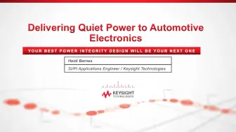
Delivering Quiet Power to Automotive Electronics
MIPI C-PHY_ What it is and How to Design it
PLTS Programming (Part4)
pyBERT_ Free software for signal-integrity analysis
Build AMI Models Faster for DDR5_LPDDR5_ PathWave ADS Memory Designer Feature De
HFSS Tutorial_ Test-Bench for SMA Connector Verification
Measuring Mutual Coupling of a 4-port 4x4 MIMO antenna with a 2-port VNA
Ansys HFSS_Circuit _ PCIe template
PCB Hybrid Boards - Design, Simulation, and Characterization
SI_PI Model Extraction Webinar - Everything You Wanted to Know But Were Afraid t
Channel_Estimation
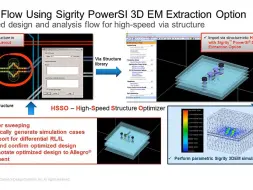
Sigrity Tech Tip_ How to Accelerate Accurate 3D Full Wave Extraction Time
ADS_ Layout Basics (Part 1)
the nanoVNA, a beginners guide to the VNA
Sigrity技術好幫手:如何輕鬆導入經3D EM優化後的3D結構到你的PCB設計工具
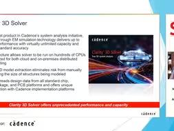
Electromagnetic Simulation of Large Chip-Package Designs Using Clarity 3D Solver