V
主页
CMOS制作工艺流程-2.5. short-channel effect 短沟道效应
发布人
-
打开封面
下载高清视频
观看高清视频
视频下载器
CMOS制作工艺流程-1. Isolation
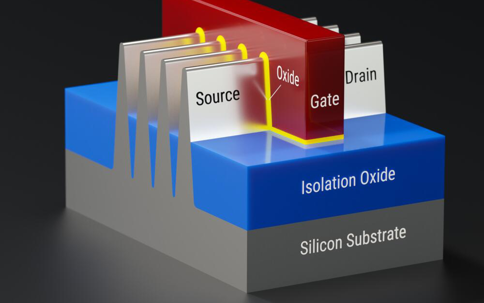
CMOS制作工艺流程-2. Transistor
二秋第四讲一笔画问题【下】
【半导体工艺】从头到尾带你彻底了解芯片半导体工艺!从半导体工艺流程介绍、IC芯片、氧化工艺、沉积工艺、CMP等等及封装工艺圈流程讲解!
3.6 An Amplifier-Less CMOS Potentiostat IC Consuming 3.7nW Power all over 129.5d
3.3 A 0.5V 6.14µW Trimming-Free Single-XO Dual-Output Frequency Reference with [
3.5 A 4mW 45pT√Hz Magnetoimpedance-Based ΔΣ Magnetometer with Background Gain Ca
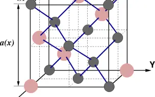
CMOS-process.7.2 MOSFET中SiGe合金的应用
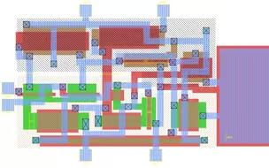
集成电路版图设计- layout design 2 - design model
集成电路版图设计 - layout design - 3. design process
CMOS制作工艺流程-5. Scaling 微缩芯片尺寸时遇到的问题
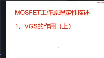
MOSFET工作原理1,VGS的作用(上)
模拟版图工程师都用什么软件?
第10课-MOSFET IV特性推导、工作区域、沟道长度调制【Ali Hajimiri大师-CMOS模拟电路设计-中文翻译版】
CMOS制作工艺流程-4. Wiring 布线
CMOS制作工艺流程-6. SOI 如何优化衬底结构
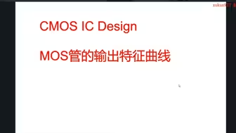
MOS管的输出特征曲线
霞课堂之霞说IGBT是如何实现优势整合的?
物竞第一课(下)
半导体物理基础概念-Semiconductor fundamentals
MOSFET-场效应管 1-MIS电容
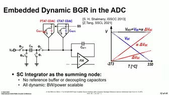
3.7 A β-Compensated NPN-Based Temperature Sensor with ±0.1°C (3σ) Inaccuracy fro
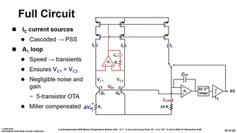
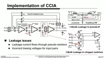
3.10 A 0.690.58-PEF 1.6nW24nW Capacitively Coupled Chopper Instrumentation Ampli
【补充】5.超声波测速
CMOS制作工艺流程-7.1. 半导体材料的性质
UNSW_ELEC_4602_Microelectronic_Design_and_Technology
详解碳化硅功率半导体的并联技术【英家必修课】
3.4 A 14b 98Hz-to-5.9kHz 1.7-to-50.8μW BWPower Scalable Sensor Interface with a
速通小学广义相对论
成电832考研2024年真题讲解/真题强化班和实验室介绍
【IC后端——寻常】STA基础之保持时间
拒绝内卷,做设计的要学点印刷工艺
CMOS IC DESIGN 关于阈值电压的讨论
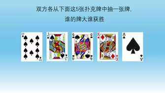
【博弈论】抽到大牌者胜,教授:你想和我换牌吗?
【半导体小白的一本正经科普】一条视频带你了解大疆造相机背后的CMOS以及CCD技术
第11课-MOSFET夹断时沟道电荷计算【Ali Hajimiri大师-CMOS模拟电路设计-中文翻译版】
突発‼️ blender 作業配信
【补充】7.运动学刹车进阶
为什么冲锋衣能挡雨?表面能-surface energy