V
主页
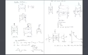
Stability Considerations in RF Amplifier Design
发布人
https://www.youtube.com/watch?v=_wkv2fKjGBU&t=590s
打开封面
下载高清视频
观看高清视频
视频下载器
CMOS VCO Design (1)
Design Example_ Class F Power Amplifier (PA)
Design of Time-to-Digital Converter (TDC)
Beyond All-Digital PLL for RF and Millimeter-Wave Frequency Synthesis
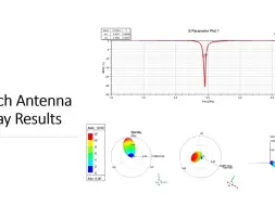
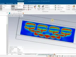
HFSS 1x2 Circular Patch Antenna Array @ 2.4 GHz
The Process Corners in VLSI Design
MOSFET (Common Source Amplifier) with Active Load Explained
Transmission Lines part 2
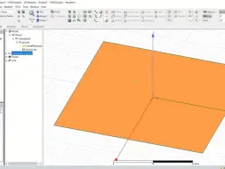
Microstrip Patch Antenna Design with HFSS
Design of NMOS in Microwind
Calculation of center and radius of stability circles and its plot on smith char
Cadence Virtuoso Design of NAND Gate Schematic (1).
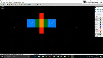
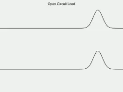
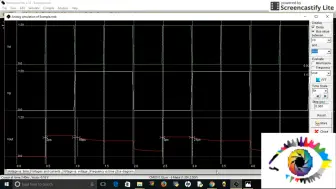
Open Circuit Load on a Transmission Line
MIT Design Example Coffee Can Doppler Radar System
Lossy Transmission Line
Design of PMOS in Microwind
CMOS inverter microwind design and simulation
Cadence Virtuoso tool for the design of CMOS inverter _ Cadence tutorial _ DC &
Cadence Layout tutorial _ Virtuoso tool for the design of CMOS inverter Layout
voltage and current propagate through transmission lines
Patch Array Antenna Design Operating at 2.45GHz
FLOORPLAN USING INNOVUS ( PART2_3) _ PHYSICAL DESIGN _ ASIC _ ELECTRONICS _ VLSI
Matched Load on a Transmission Line
Create Delay Using Systick Timer and PLL
Visualizing RF Standing Waves on Transmission Lines
Embedded Flash Memory
Gain and Phase Margins Explained
Cross Coupled Pair Part 2
Latch Up in CMOS, Latch up in CMOS Inverter
Open-Loop vs. Closed-Loop Transfer Function
180N. Latch dynamics, latched comparator
Understanding the Z-Transform
Cross Coupled Pair Part 1
Memristive Materials and Devices for Neuromorphic Computing
How to make layouts in Microwind software explained with an example of CMOS inve
Understanding SPI
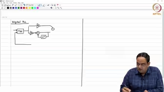
Introduction to Digital PLL
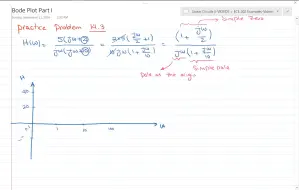
Bode Plot EXAMPLE
4x1 and 1x2 Rectangular Patch 2.4 GHz Antenna Array 2.4 to 4.2 THz SiO2 graphene