V
主页
Cadence Virtuoso tool for the design of CMOS inverter _ Cadence tutorial _ DC &
发布人
https://www.youtube.com/watch?v=_1b-n0m3PX4
打开封面
下载高清视频
观看高清视频
视频下载器
Cadence Layout tutorial _ Virtuoso tool for the design of CMOS inverter Layout
CMOS VCO Design (1)
CMOS inverter microwind design and simulation
Latch Up in CMOS, Latch up in CMOS Inverter
Logic Synthesis of RTL _ Synopsys Design Compiler _ Synopsys DC _ dc_shell _ DC
Cadence Virtuoso__ Layout of NAND Gate __ Part-2.
Cadence Virtuoso Design of NAND Gate Schematic (1).
Shahar Kvatinsky Memristorbased Logic Circuit Design_360p
Cadence Tutorial for Ring Oscillator
VLSI lab_ cmos inverter using DSCH and Microwind
Design of input_output matching network for maximum gain transistor amplifier by
Design Example_ Class F Power Amplifier (PA)
Stability Considerations in RF Amplifier Design
CMOS Transmission Gate, Working of CMOS Transmission Gate
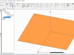
Design of inset-feed microstrip antenna at 2.4 GHz
模拟集成电路设计8-运算放大器的设计
FLOORPLAN USING INNOVUS ( PART2_3) _ PHYSICAL DESIGN _ ASIC _ ELECTRONICS _ VLSI
Amplifiers_ Bilateral Design
Microwind_intro_meeting ELEC3285 integrated circuit design UoLeeds
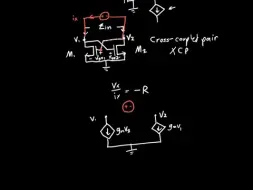
Cross Coupled Pair Oscillator Part 2
How to Design an RF Power Amplifier_ Class F
Cross Coupled Pair Oscillator Part 1
Cadence为什么比AD上手难?
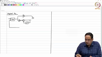
Design of Time-to-Digital Converter (TDC)
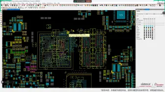
01 突破技术瓶颈:Cadence Allegro X 23.1革新揭秘
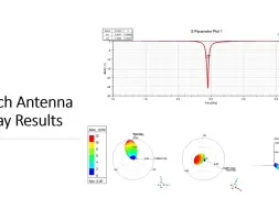
Patch Array Antenna Design Operating at 2.45GHz
MIT Design Example Coffee Can Doppler Radar System
Microstrip Patch Antenna Design with HFSS
cadence virtuso入门
Understanding the Z-Transform
04 突破技术瓶颈:布局优化与高效技巧
Cross Coupled Pair Part 1
03 突破技术瓶颈:阻抗控制与层叠设计艺术
Open-Loop vs. Closed-Loop Transfer Function
2024嵌入式物联网Alot智能电车防盗系统项目
HFSS 1x2 Circular Patch Antenna Array @ 2.4 GHz
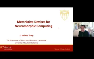
Prof. J. Joshua Yang, Memristive Devices for Neuromorphic Computing
MOSFET (Common Source Amplifier) with Active Load Explained
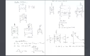
180N. Latch dynamics, latched comparator
基准电压源_理论