V
主页
京东 11.11 红包
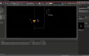
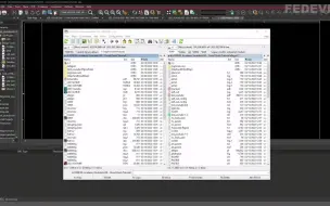
01-OrCAD and Cadence Allegro示意图-004创建360R电阻器示意图符号
发布人
打开封面
下载高清视频
观看高清视频
视频下载器
01-OrCAD and Cadence Allegro示意图-003创建1x2标头示意图符号
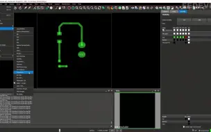
02-OrCAD and Cadence Allegro 足迹-005创建1x2标头足迹
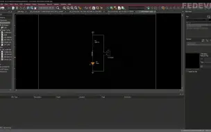
01-OrCAD and Cadence Allegro 示意图-005创建LED示意图符号
02-OrCAD and Cadence Allegro 足迹-004创建VIA
02-OrCAD and Cadence Allegro 足迹-007创建0805电阻器足迹.mp4
01-OrCAD and Cadence Allegro 示意图-006图纸示意图
02-OrCAD and Cadence Allegro 足迹-003为LED创建SMD焊盘
04 OrCAD和Cadence Allegro输出-004生成拣货和放置文件
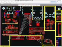
03 OrCAD和Cadence Allegro PCB布局-002组件放置
04 OrCAD和Cadence Allegro输出-005打印示意图
01-OrCAD and Cadence Allegro示意图-002开始新项目
02-OrCAD and Cadence Allegro Footprints-009修复警告并运行DRC
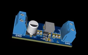
03 OrCAD和Cadence Allegro PCB布局-007精加工PCB
03 OrCAD和Cadence Allegro PCB布局-006编辑示意图和更新PCB
03 OrCAD和Cadence Allegro PCB布局-001启动新PCB
03 OrCAD和Cadence Allegro PCB布局-003设置规则和堆栈
02-OrCAD and Cadence Allegro 足迹-006创建0603 LED足迹.mp4
04 OrCAD和Cadence Allegro输出-002生成NC钻孔文件
【自制图传遥控器】坏消息缝合怪,好消息全缝上了
基于Cadence 16.6的Allegro入门教程
Part2-800MHz 45W 射频功率放大器的快速实现
1小时入门PCB,保姆级教程来了(STM32/RK3568学习资料包)
嘉立创第一次pcb培训
为什么三极管做推免电路时,经常用上N下P结构,而不用上P下N的结构
应急启动电源 140W主板 上篇
开关电源TPS54302的5V输出电路设计
PCB锐角走线有啥危害?
Altium designer-10月11日四层板PCB板练习
【硬核】手搓电容屏-第一版
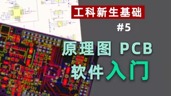
想学电子DIY?适合小白的原理图、PCB绘制软件入门教程
10.10、HDMI PCB设计之走线
LED电路中的电阻有什么作用
手把手教你做【WIFI控制器】③:PCB布局技巧
PCB蓝胶工艺,你了解多少呢
高频pcb板和普通pcb板有什么区别
板厂测阻抗做Coupon条,测S参数做什么条?
Cadence 培训内容——任您选用
【DIY】自制4bitCPU-TD4-74电路搭建-开源
【FPGA硬件设计教程】布局布线第五期(电源树layout)
PCB 工艺边是什么?