V
主页
京东 11.11 红包
[Logic Device Part1] High-k Metal Gate HKMG
发布人
https://www.youtube.com/watch?v=l9VwY0aN5uY&t=2s 该视频脚本介绍了高K金属栅极技术在半导体制造中的重要性,以及金属栅极对晶体管性能的影响。讨论了栅极电容的影响和金属合金的稳定性。还提到了多阈值电压实施和Gate Last工艺的优势。最后,介绍了通过3D器件结构克服Boltzmann极限的方法,以提高半导体器件的性能和效率。
打开封面
下载高清视频
观看高清视频
视频下载器
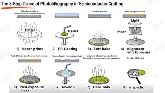
[Photolithography Part1] Track (Coating & Develop)
[Thin Film Part1] Stress and Strain
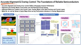
[Photolithography Part3] Alignment & Overlay
[Thin Film Part7] BEOL Interconnect 1
[EUVL Part1] From the Beginning to HVM
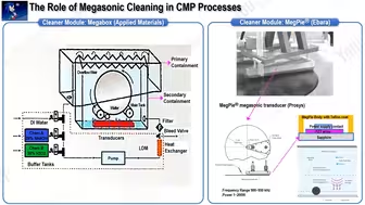
1-[CMP Part1] CMP Introduction (1 of 2)
[Photolithography Part6] Photomask (2 of 2)
Introduction to Semiconductor Physics and Devices
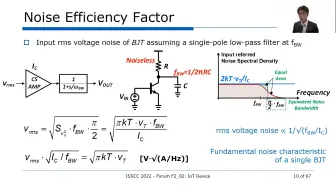
F2.Sensor.Interface.Analog.and.Mixed.Signal.Circuits.for.Miniaturized.IoT.Device
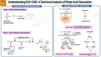
[EUVL Part5] EUV Resist
伯克利-高级模拟集成电路-EECS240-lecture2(英文字幕修正)
[Photolithography Part5] Multiple Patterning Technology (MPT)
[Thin Film Part4] PVD Basics
[Thin Film Part2] Vacuum Basics
[EUVL Part3] EUV Mirror
[Photolithography Part4] CD Measurement & Control
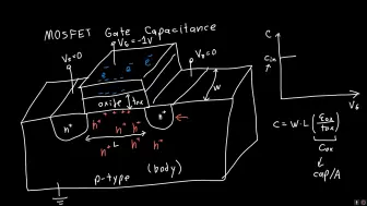
MOSFET Gate Capacitance Part 2
3-[CMP Part2] CMP Mechanics (1 of 2)
[EUVL Part4] EUV Mask
[Thin Film Part8] BEOL Interconnect 2
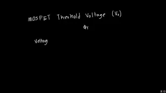
MOSFET Threshold Voltage Explained
[EUVL Part2] ASML EUV Light Source
[Fab Part1] All About Silicon Wafers
[Photolithography Part7] Photoresist
[Thin Film Part5] CVD Basics
[Thin Film Part6] ALD Basics
Ep35 Semiconductor Engineering 半導體製程與整合(共36集)台灣清華大學吳永俊教授!此影片僅供教學非營利使用!
SC2.Ultra.High.Data.Rate.ADCs.and.DACs.Architectures.and.Implementations
半导体基本工艺简答(面试/复试向)
[Photolithography Part6] Photomask (1 of 2)
Ep36 Semiconductor Engineering 半導體製程與整合(共36集)台灣清華大學吳永俊教授!此影片僅供教學非營利使用!
【半导体工艺】目前B站最全最细的半导体工艺全套教程。从头到尾带你彻底了解芯片半导体工艺!让你少走99%的弯路,这还学不会,我退出机械圈!
MOSFET Body Effect Explained
4-[CMP Part2] CMP Mechanics (2 of 2)
【黑马】集成电路和嵌入式开发2024
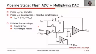
SC3.High.Precision.and.Low.Power.ADCs
2-[CMP Part1] CMP Introduction (2 of 2)
Ep1 Semiconductor Engineering 半導體製程與整合(共36集)台灣清華大學吳永俊教授!此影片僅供教學非營利使用!
Law of the Junction
ESSCIRC 2024 Circuit Insights 4-Data Converters