V
主页
京东 11.11 红包
The Importance of Miniaturization: Electronic Phenomena at the Nanoscale
发布人
Abstract: Multiple research articles fabricate large electronic devices (with lateral sized >10 µm2) and claim that the behaviors observed are “promising” for applications like data storage or computing. In small-size devices, the number of local defects in the materials can be remarkably different, which almost always affects switching voltages, energies and times, as well as state resistances may be remarkably different than in larger devices, which also affects yield, variability and reliability. Hence, the fact that a large device (>10 µm2) shows whatever performance does not imply that a small device (<0.01 µm2) with identical materials composition will also exhibit it. I will show multiple methods to characterize the electronic properties of different materials and devices at the nanoscale and describe some of the properties I have analyzed in metal-oxides, graphene, molybdenum disulfide, hexagonal boron nitride, and nanowires. I will describe the setups that I have developed in order to carry out these studies, with special emphasis in conductive atomic force microscopy. The main properties that I will discuss are related to leakage current, dielectric breakdown and resistive switching in thin dielectrics, as well as piezoelectricity in two-dimensional materials and nanowires. Biography: Mario Lanza got a PhD in Electronic Engineering in 2010 at Universitat Autonoma de Barcelona. In 2010-2011 he was NSFC postdoc at Peking University, and in 2012-2013 he was Marie Curie postdoc at Stanford University.Now he is an Associate Professor of Materials Science and Engineering at the KAUST in Saudi Arabia. Prof. Lanza has published over 120 research papers, including two Science, five Nature Electronics and 10 Advanced Materials, and has registered four patents. He is a editor-in-chief of the journal Microelectronic Engineering (Elsevier), he is also the chair of the Nanotechnology Committee of the Electron Devices Society.
打开封面
下载高清视频
观看高清视频
视频下载器
原子力显微镜电性测量关于C-AFM; EFM; KPFM 的介绍讲解
磁力显微镜(MFM) - 原子力显微镜
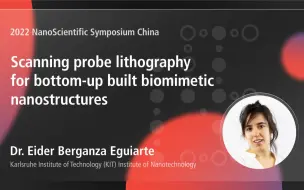
Scanning Probe Lithography for bottom-up built biomimetic nanostructures
AFM网络讲座系列第二讲_ 原子力探针显微术基础及其研展_-核心基础工作模式及其进展
网络讲座Live Demo:开尔文探针力显微镜 (KPFM) 原理及应用介绍
网络讲座:一种可印刷、可重构的虎符式交流电致发光器件
Quantitative Imaging of Localized Functionalities at the Nanoscale
原子力显微镜(AFM)的工作原理
Single-molecule chemical reactions probed by Atomic Force Microscopy
导电原子力显微镜(C-AFM)在先进纳米电子学中的应用
(油管)通过边带开尔文探针力显微镜(KPFM)进行表面电势成像
(youtube油管)新型表面活性剂的设计
现场演示:使用KPFM进行表面电势映射的比较研究
转角二维材料的堆垛表征及调控
二维多铁材料中的高效磁电耦合调控
Atomic insights into the interfacial ion-water interaction
扫描隧道显微镜(STM)最新技术和Park SmartScan
Park原子力显微镜 AFM使用操作说明
网络讲座:基于扫描电化学显微镜(SECCM)的纳米级电化学研究
[AFM入门]原子力显微镜的基础原理(完整视频)
Park原子力显微镜公司介绍
PFM在层状范德瓦尔斯铁电体中的应用
Park NX-Wafer: 晶圆厂唯一具有自动缺陷检测的原子力显微镜
用原子力显微镜研究热电材料中的缺陷物理
(youtube 油管)压电力显微镜(PFM)的高级应用
自动化AFM在半导体先进制程的应用进展
原子力显微镜操作技巧
原子力显微镜缺陷检测的相关应用
Park SmartScan™ - AFM成像技术中的一键点击革命
SEMICON West Park CEO 新品介绍采访视频
AFM网络讲座系列第三讲:原子力探针显微术基础及其应用进展_- 功能化原子力探针显微术
原子力显微镜助力研究分层材料
生活中甜蜜的一面:如何轻松地对软样品(如巧克力)进行纳米力学原子力显微镜测量
原子力显微镜用于体相异质结太阳能电池
SmartLitho™ Creating nanometer sized structures with ease
近场光学显微术及其应用
Park NX10 全自动化高端原子力显微镜
导电原子力显微镜(C-AFM)在二维材料及纳_米电子器件中的应用
(Youtube油管)纳米技术在塑料包装领域中的应用
一般环境下原子力显微镜观察单分子存在的挑战