V
主页
1.8. Mass action law
发布人
打开封面
下载高清视频
观看高清视频
视频下载器
12.9. NOR FLASH
12.11. SRAM cell
6.8. I_O pipelining
1.6. Doping
7.8. Etching & CMP
4.4. Parasitic delay
1.4. Carrier concentration
6.9. Internal pipelining
2.2. Preliminaries of logic
1.12. PN junction
2.1. PMOS Transistors
4.8. Complications of optimization
7.9. Exposure strategies
7.3. Account of materials
12.18. Column decoders
6.5. Imperfect clocks and hold time
7.7. Photoresist coating, baking, & development
6.2. CMOS latches
6.6. Dynamic latches & registers
5.7. NP logic
4.6. Optimizing logic
2.3. Scaling MOSFET
3.7. Dynamic power
12.12. SRAM read and write
12 21 Row decoders design using logical effort
4.7. Analyzing optimal solutions
12.17. DRAM read, write, and refresh cycles
5.8. Domino logic
12.13. Sense amplifiers
12.5. NAND ROM
12.15. Three transistor DRAM
2.7. Enhancement load inverter
6.7. Basics of pipelining
12.6. Delay in NAND ROM
2.6. RTL
7.6. CVD, PVD, & oxidation
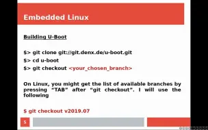
Embedded Linux _ Introduction To U-Boot _ Beginners
1.9. Drift
7.5. Ion implantation & diffusion
2.11. Complex enhancement synthesis