V
主页
2.9. Enhancement load NOR
发布人
enhanced load nor
打开封面
下载高清视频
观看高清视频
视频下载器
2.7. Enhancement load inverter
2.8. Enhancement load VTC
12.9. NOR FLASH
12.13. Sense amplifiers
3.9. CMOS NAND and NOR
12.11. SRAM cell
2.12. Complex enhancement analysis
2.11. Complex enhancement synthesis
2.10. Enhancement NAND gate
12.12. SRAM read and write
6.8. I_O pipelining
4.2. Inverter chains
6.9. Internal pipelining
6.7. Basics of pipelining
1.6. Doping
4.6. Optimizing logic
7.8. Etching & CMP
12.4. Delay in NOR ROM
4.8. Complications of optimization
4.5. Logical effort
7.9. Exposure strategies
1.12. PN junction
1.4. Carrier concentration
1.5. Intrinsic silicon
4.4. Parasitic delay
3.7. Dynamic power
6.1. Sequential CMOS
4.7. Analyzing optimal solutions
6.10. Setup-time violations
6.6. Dynamic latches & registers
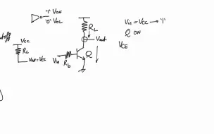
2.5. Bipolar logic
7.4. Czochralsky process and wafer preparation
7.2. Photolithography
7.7. Photoresist coating, baking, & development
2.3. Scaling MOSFET
1.7. Extrinsic silicon
12.5. NAND ROM
6.5. Imperfect clocks and hold time
2.2. Preliminaries of logic
5.7. NP logic